- 您现在的位置:买卖IC网 > Sheet目录1993 > DS1339AU+ (Maxim Integrated Products)IC RTC I2C W/ALARM 8USOP
DS1339A
Low-Current, I2C, Serial Real-Time Clock
3
Maxim Integrated
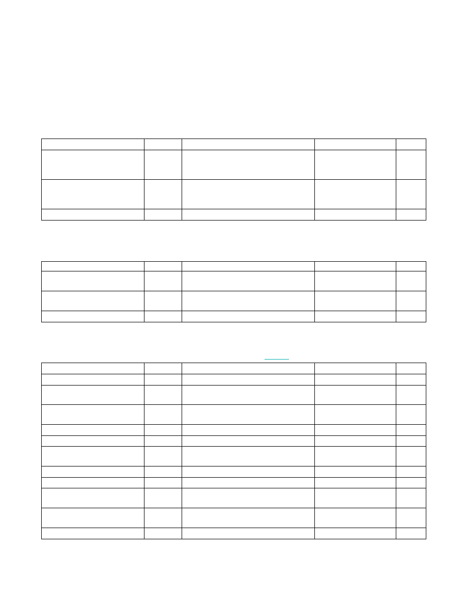
DC ELECTRICAL CHARACTERISTICS (continued)
(VCC = MIN to MAX, VBACKUP = MIN to MAX, TA = -40NC to +85NC, unless otherwise noted.) (Note 2)
DC ELECTRICAL CHARACTERISTICS
(VCC = 0V, VBACKUP = MIN to MAX, TA = -40NC to +85NC, unless otherwise noted.) (Note 2)
AC ELECTRICAL CHARACTERISTICS
PARAMETER
SYMBOL
CONDITIONS
MIN
TYP
MAX
UNITS
Trickle-Charger Resistor Register
10h = A6h, VCC = Typ,
VBACKUP = 0V
R2
2000
I
Trickle-Charger Resistor Register
10h = A7h, VCC = Typ,
VBACKUP = 0V
R3
4000
I
VBACKUP Leakage Current
IBKLKG
-100
25
200
nA
PARAMETER
SYMBOL
CONDITIONS
MIN
TYP
MAX
UNITS
VBACKUP Current EOSC = 0,
SQW Off
IBKOSC
(Note 8)
300
600
nA
VBACKUP Current EOSC = 0,
SQW On
IBKSQW
(Note 8)
500
1100
nA
VBACKUP Current EOSC = 1
IBKDR
10
200
nA
PARAMETER
SYMBOL
CONDITIONS
MIN
TYP
MAX
UNITS
SCL Clock Frequency
fSCL
0.03
400
kHz
Bus Free Time Between a STOP
and START Condition
tBUF
1.3
F
s
Hold Time (Repeated) START
Condition
tHD:STA
(Note 9)
0.6
F
s
Low Period of SCL Clock
tLOW
1.3
F
s
High Period of SCL Clock
tHIGH
0.6
F
s
Setup Time for a Repeated
START Condition
tSU:STA
0.6
F
s
Data Hold Time
tHD:DAT
(Notes 10, 11)
0
0.9
F
s
Data Setup Time
tSU:DAT
(Note 12)
100
ns
Rise Time of Both SDA and SCL
Signals
tR
(Note 13)
20 +
0.1CB
300
ns
Fall Time of Both SDA and SCL
Signals
tF
(Note 13)
20 +
0.1CB
300
ns
Setup Time for STOP Condition
tSU:STO
0.6
F
s
发布紧急采购,3分钟左右您将得到回复。
相关PDF资料
DS1339C-2#
IC RTC I2C W/ALARM 16-SOIC
DS1340Z-33/T&R
IC RTC I2C W/CHARGER 3.3V 8-SOIC
DS1340Z-3
IC RTC I2C W/CHARGER 3V 8-SOIC
DS1341T+
IC RTC I2C W/ALARM 6TDFN-EP
DS1344D-33+
IC RTC SPI 3.3V 14TDFN-EP
DS1347T+
IC RTC/CALENDAR SPI 8TDFN
DS1371U+C01
IC BINARY COUNTER 32-BIT 8-USOP
DS1372U+T&R
IC BINARY COUNTER 32-BIT 8-USOP
相关代理商/技术参数
DS1339AU+T
功能描述:实时时钟 1.8-3.3V Serial RTC RoHS:否 制造商:Microchip Technology 功能:Clock, Calendar. Alarm RTC 总线接口:I2C 日期格式:DW:DM:M:Y 时间格式:HH:MM:SS RTC 存储容量:64 B 电源电压-最大:5.5 V 电源电压-最小:1.8 V 最大工作温度:+ 85 C 最小工作温度: 安装风格:Through Hole 封装 / 箱体:PDIP-8 封装:Tube
DS1339BU+
功能描述:实时时钟 SERIAL RTC 1.8-3.3V C 1.8-3.3V HESR USOP RoHS:否 制造商:Microchip Technology 功能:Clock, Calendar. Alarm RTC 总线接口:I2C 日期格式:DW:DM:M:Y 时间格式:HH:MM:SS RTC 存储容量:64 B 电源电压-最大:5.5 V 电源电压-最小:1.8 V 最大工作温度:+ 85 C 最小工作温度: 安装风格:Through Hole 封装 / 箱体:PDIP-8 封装:Tube
DS1339BU+T
制造商:Maxim Integrated Products 功能描述:SERIAL RTC 1.8-3.3V HESR USOP TRL - Tape and Reel 制造商:Maxim Integrated Products 功能描述:IC RTC I2C W/ALARM 8UMAX
DS1339C-2
功能描述:实时时钟 I2C Serial RTC RoHS:否 制造商:Microchip Technology 功能:Clock, Calendar. Alarm RTC 总线接口:I2C 日期格式:DW:DM:M:Y 时间格式:HH:MM:SS RTC 存储容量:64 B 电源电压-最大:5.5 V 电源电压-最小:1.8 V 最大工作温度:+ 85 C 最小工作温度: 安装风格:Through Hole 封装 / 箱体:PDIP-8 封装:Tube
DS1339C-2-
制造商:MAXIM 制造商全称:Maxim Integrated Products 功能描述:I2C Serial Real-Time Clock
DS1339C-2#
功能描述:实时时钟 I2C Serial RTC RoHS:否 制造商:Microchip Technology 功能:Clock, Calendar. Alarm RTC 总线接口:I2C 日期格式:DW:DM:M:Y 时间格式:HH:MM:SS RTC 存储容量:64 B 电源电压-最大:5.5 V 电源电压-最小:1.8 V 最大工作温度:+ 85 C 最小工作温度: 安装风格:Through Hole 封装 / 箱体:PDIP-8 封装:Tube
DS1339C-2+
制造商:Maxim Integrated Products 功能描述:REAL TIME CLOCK SERL 16SOIC W - Bulk
DS1339C-3
功能描述:实时时钟 RoHS:否 制造商:Microchip Technology 功能:Clock, Calendar. Alarm RTC 总线接口:I2C 日期格式:DW:DM:M:Y 时间格式:HH:MM:SS RTC 存储容量:64 B 电源电压-最大:5.5 V 电源电压-最小:1.8 V 最大工作温度:+ 85 C 最小工作温度: 安装风格:Through Hole 封装 / 箱体:PDIP-8 封装:Tube